Using the serial port - part 1
- Introduction
- Sample BASIC program
- Closer look at the program
- Troubleshooting
- Closer look at the documentation
- Pinouts and flow control
- Next steps
- References
Introduction
The Alphatronic P2 has actually two serial ports: One, that is used to connect a line printer. And I already used that one with the null modem cable I created. This serial port only has the TX and RX lines connected and doesn’t support flow control. It is actually implemented by using the SOD and SID pins of the 8085 CPU.
But the Alphatronic has an additional serial port using a dedicated 8251. This is connected to the back with a 25-pin connector, like the other one. But this time, all the extra signals like DSR/DTR, CTS/RTS are connected as well, allowing to use hardware flow control.
Sample BASIC program
The “Alphatronic Systemhandbuch” (available from the Computermuseum of the University of Stuttgart) contains a sample BASIC program to access and use the serial port on page 125 (chapter 4.4.3). Here it is:
V 24 DEMOPROGRAMM
 10     REM V 24 DEMOPROGRAMM
 20     PRINT CHR$(12)
 30     GOSUB 510 INIT USART
 40     INPUT "SENDER ODER EMPFAENGER (S/E)"; S$
 50     PRINT
 60     PRINT CHR$(28)
 70     PRINT "*** ZUM AENDERN DER ZUORDNUNG";
 80     PRINT "(SENDER <---> EMPFAENGER) '*' EINGEBEN ***"
 90     PRINT CHR$(18)
100     FOR I = 1 TO 3000 : NEXT
110     PRINT
120     IF S$ = "E" GOTO 320
130     IF S$ <> "S" GOTO 40
140     '********** TRANSMITTER **********
150     PRINT "********** SENDER **********"
160     PRINT
170     A$ = ""
180     OUT 5,&H13
190     WHILE (INP(5) AND 128) = 0
200     PRINT "WAIT ON R";
210     WEND
220     PRINT
230     WHILE A$ <> "*"
240     A$ = INPUT$(1) : PRINT A$;
250     C = ASC(A$)
260     OUT 5,&H13
270     WHILE (INP(5) AND &H1) = 0 : WEND
280     OUT 4,C
290     WEND
300     PRINT
310     OUT 5,&H10
320     '********** RECEIVER **********
330     PRINT "********** EMPFAENGER **********"
340     PRINT
350     ZE = &H0
360     WHILE (INP(5) AND 128) = 0
370     PRINT "WAIT ON T";
380     WEND
390     PRINT
400     WHILE (INP(5) AND 128) = 0 : WEND
410     OUT 5,&H36
420     WHILE CHR$(ZE) <> "*"
430     ZE = &H0
440     WHILE (INP(5) AND &H2) = 0 : WEND
450     ZE = INP(4)
460     PRINT CHR$(ZE);
470     WEND
480     PRINT
490     OUT 5,&H10
500     GOTO 140
510     '********** INIT USART **********
520     OUT 5,&H91
530     OUT 5,&H40
540     OUT 5,&H4A 'ASYN. NO PARITY, 4800 BAUD
550     ' 1 STOP BITS, 7 BITS
560     OUT 5,&H10
570     RETURN
I tried this out, but unfortunately I was not able to receive anything on the serial cable when the Alphatronic was supposed to set a character. It turns out, it is stuck in a while loop waiting for some signal to happen.
Closer look at the program
So, let’s have a closer look, what actually is done here.
It first starts by clearing the screen (PRINT CHR$(12)) and then jumps to the
initialization routine (GOSUB 510).
Initialization
There we write out 4 bytes to the I/O port 5. The I/O port with address 5 is connected (hopefully) in such a way, that it asserts the “C/^D” line to send a control byte to the 8251. Initializing this chip is a bit tricky: After hard reset, the chip is in idle state and expects a mode instruction. Once the mode instruction has been received, it expects from now on only command instructions. The mode instruction is used e.g. to select the baud rate. The command instruction is used to control the transmitter/receiver. But when you want to initialize the chip, you could assume, it is in idle state. But you are not sure. If it is in idle mode, then the firs byte would be interpreted as mode instruction. It’s even more complicated: If the chip is instructed to use synchronous mode, then it expects two more bytes (“sync character 1” and “sync character 2”) before it expects command instructions. With a specific command instruction, you can execute a soft reset - bringing the chip back to idle state, so that it accepts once again a mode instruction. The datasheet for the 8251 suggests in the note on “Internal Reset on Power-up”, to load three 00H consecutively into the device as control bytes. This would configure the chip into sync mode and writes two dummy 00H sync characters. After that an internal reset command (40H) can be sent and the chip is definitively in idle state.
What does the sample program do? It sends first &H91, then &H40. Aha, this
&H40 seems to be the internal reset command. Then it sends &H4A. If this is
interpreted as a mode instruction, then this means: the two lowest bits define
the baud rate or sync mode. Here we have 10 and that means: async mode with
16x baud rate factor. The next two bits are 01, which means 7 bits character
length. Then no parity is configured. And one stop bit.
So, this matches what the comment says. Good. The baud rate factor is somehow
connected to the baud rate. According to the comment, we should get 4800 baud.
The 7 bits is quite an old format, more common nowadays is 8n1, which means
8 bits characters, no parity bit, 1 stop bit. That would be then &H4E for
the mode instruction.
The last byte written out is &H10. That’s the first command instruction and
simply resets the error flags.
Sender
Ok, let’s go on and assume, we entered a “S”, so that we are the sending side
of the connection. Then we don’t execute the goto in line 120 and we go on
in line 140. In line 180, we output &H13 to the chip. This is now a command
instruction and means: Enable the transmitter, assert the DTR line and reset
any error flags. Sounds good, transmitter is enabled.
Then in line 190 we repeatedly read from the I/O port. When reading from the 8251, we get back the status. And we check the 8th bit (128): That is the DSR (Data Set Ready) line. We wait, while this line is zero. Once the line is asserted, then we end the while loop. So, that’s part of the hardware flow control protocol. My receiver needs to assert this line to indicate it is ready to receive data.
I could see, that this line actually works: With cutecom you can select “no hardware flow control” and the you have two checkboxes to manually control the lines “RTS” and “DTR”. And this works: The BASIC program repeatedly prints out “WAIT ON R” until I select “DTR”.
So we come to line 240, where one character is requested from the keyboard.
Once you press a key the character is in A$. That’s supposedly a string
and the first character is taken into variable C. Then in line 260
we again enable the transmitter and clear the error flags and then
we wait in a while loop for the first bit in the status register: This is
the TxRDY status bit. This just checks, that the data buffer in the chip is
empty and we can put a new byte into the chip to be sent.
So, if all is fine, we actually send out one byte in line 280 by writing to the I/O port 4. Then we repeat in line 230 and ask for another keyboard press.
When I tried out the program, I could actually now enter a second character but now the program is stuck in line 270 - as the data buffer is not empty anymore. And for some reason it seems to become never empty anymore. This matches the observation, that I don’t receive any data. So, for some reason, the transmitter is not sending the data. I could verify this by printing out the status register. The first bit never becomes zero, so the data buffer is never empty. For the first character, the data buffer was empty. Supposedly one character is put into the buffer with line 280.
Assuming we entered a “*”, then the while loop started in line 230 ends
and we continue in line 300. In line 310 we issue one more command: &H10.
This just resets the error flags in the status register.
And we fall through to line 320, which is the receiver part of the program.
Receiver
For completeness, let’s look at how the receiver code works. I only tested it quickly, but I couldn’t see any character appearing. But this part has for me a lower priority. I first want to concentrate bringing the transmitter side to transmitting and the we can go on. But anyway.
First we wait until the 8th bit (“128”) in the status register is zero in line 360. This is again the DSR (Data Set Ready) bit. So we wait that the other endpoint is ready for communicating. While waiting, we would print out “WAIT ON T”.
In line 400, we do the same check again. Not sure why. Maybe just to be sure, it’s still the case and nothing changed.
In line 410 we issue the command &H36. This is in binary 0011 0110 and means:
Assert DTR (Data Terminal Ready), enable the receiver, reset the error flags
and assert RTS (Ready to send). That makes sense: We start the receiver in
the chip.
Then in line 420 we wait for the 2nd bit in the status - this is the RxRDY bit. So we wait until the chip is ready to receive the next character or actually, until the next character has actually been received and is ready for us to fetch, which we do in line 450. However, that apparently never happened. We are stuck here, too.
Assuming the program would receive a asterisk “*” character, then the while
loop would end at line 470 and we issue once again &H10 to basically
disable transmitter and receiver and reset the error flags before jumping
back to the sender side at line 140.
Troubleshooting
Helpful in troubleshooting is to now, where exactly we got stuck. The basic interpreter can be interrupted with the “Control” button as explained in the user manual:

When you press this key and then the C key, then you can interrupt a running BASIC program. The interpreter will print out the line at which the program has been interrupted.
That way, I found out, that the program got stuck always in line 270.
You can also run a single line program and continually print out the status register
like so: WHILE (1=1) : S=INP(5) : PRINT S : WEND. When then toggling the
DTR line in cutecom, you can see the result directly on the screen. So that
signal line is connected correctly through my self made null modem cable.
I tried out also to use the extend initialization with the three zero bytes. But that also didn’t change anything. Still no transmission is occurring.
By the way: The keyboard also has the reset key:

This will perform a soft reset. That means, that the memory is not erased, so the
BASIC interpreter and the currently running program is still in the memory. You
don’t need to insert the floppy to boot from, you can just enter G to start
the BASIC interpreter again and then enter RUN to start the BASIC program again.
No need to load again neither the BASIC interpreter nor the program.
But conclusion for now: Neither transmitter nor receiver is working. There is no clear indication why it doesn’t work.
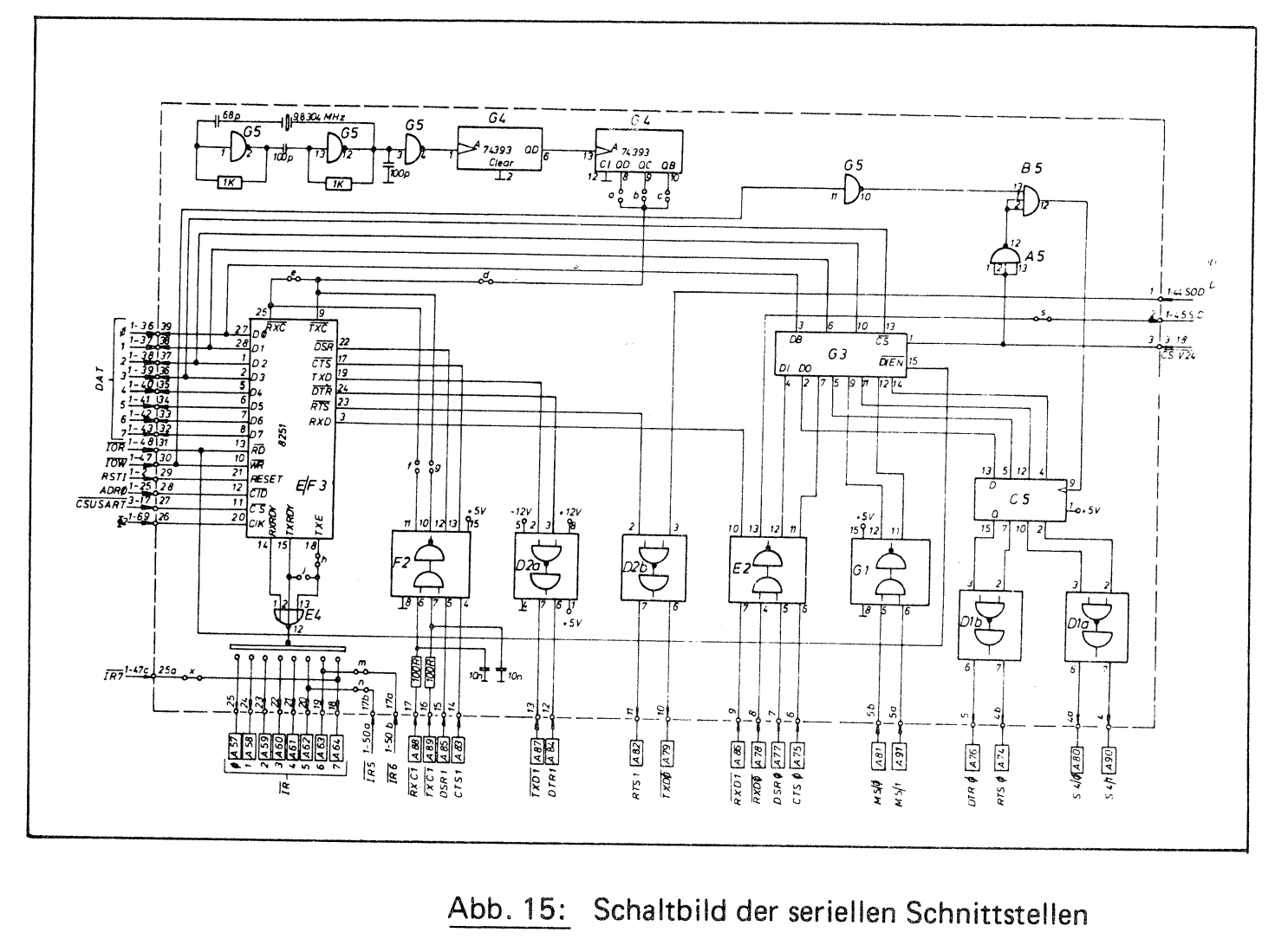
Closer look at the documentation
It’s time to have a closer look at the documentation: There is says, that we
have a couple of soldered jumpers on the CPU board, where the 8251 is sitting.
These jumpers control the clock frequency that is used for transmitting or
receiving. The factory default setting is also described: Jumpers “a” and “c”
are open, while jumper “b” is closed. With a baud rate factor of “16” - which
we used while initializing the chip with &H4A earlier - this should result
in the frequency of 4800 x 16 = 76.8 kHz. Is this correct? There is also
a quartz on the board that is used according to the circuit diagram and the
soldered jumpers. The quartz has the frequency of 9.8304 MHz and is divided
a couple of times using binary counters (74393). It’s first divided by 16
which results in 614.4 kHz. Then with jumper “b” closed, it’s divided again
by 8 and we get 76.8 kHz. That would match the documentation.
But are the jumpers still in factory default setting?
And there are more jumpers: There are two more control lines available at the connector - TxC and RxC. These are the Transmitter Clock and Receiver Clock lines connected to pin 15 and 17 of the 25-pin connector. In my null modem cable I didn’t use these, so they are unconnected. But according to the documentation for the jumpers “d” and “e” (closed) and “f” and “g” (open) the internal baud rate should be used. These lines supposedly can be used when you have an external clock. The circuit diagram also confirms this: With “d” and “e” closed the 76.8kHz clock is connected to the /RxC and /TxC pins of the 8251. And with “f” and “g” open, the RxC and TxC lines are effectively disconnected.
Here’s the circuit diagram, found on page 107 in the “Systemhandbuch” of the Alphatronic:
Now it’s time to look at the real board to check the soldered jumpers. At first glance, I didn’t find the jumpers, but I found them now on the back of the board - on the opposite site of the 8251.
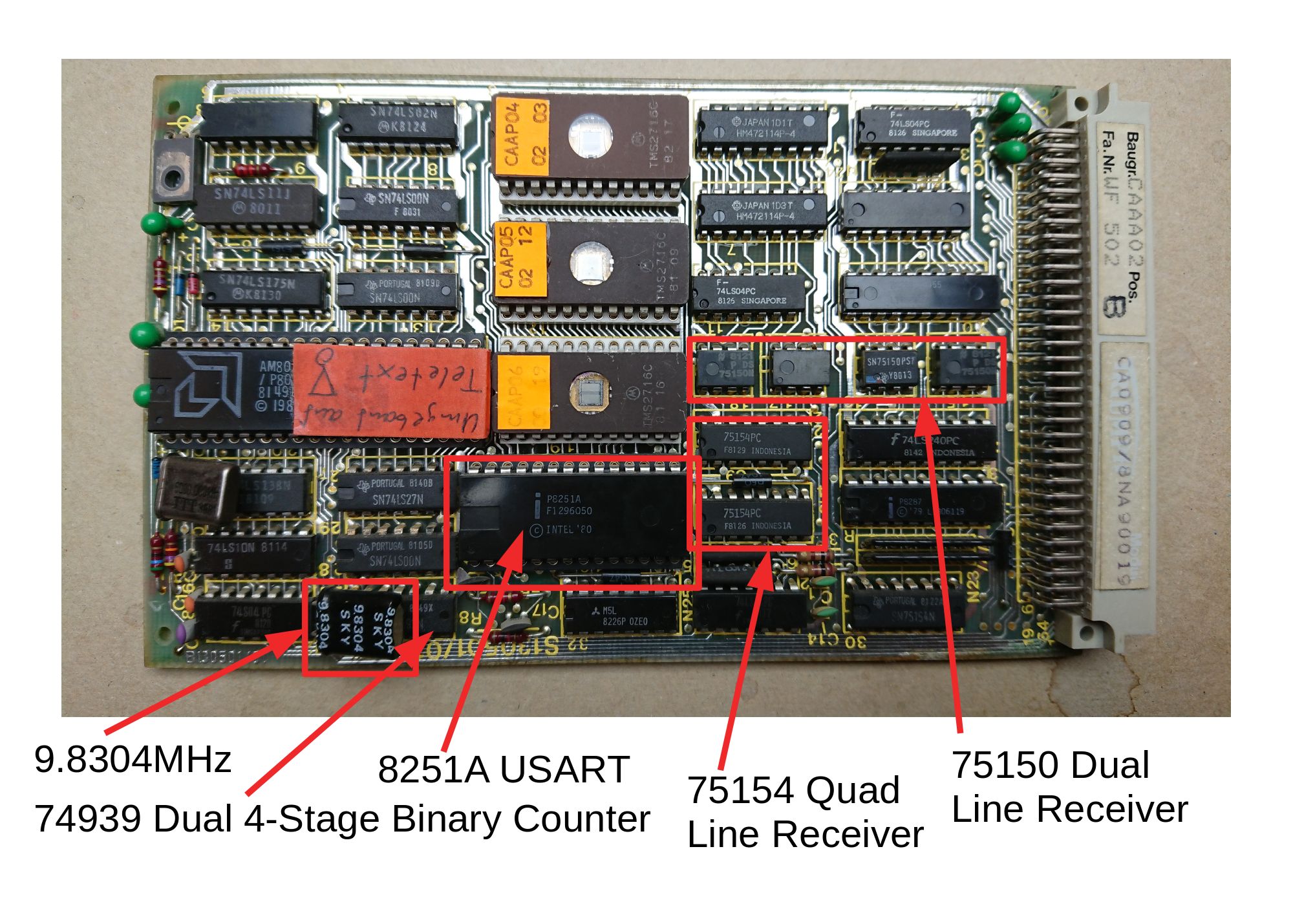
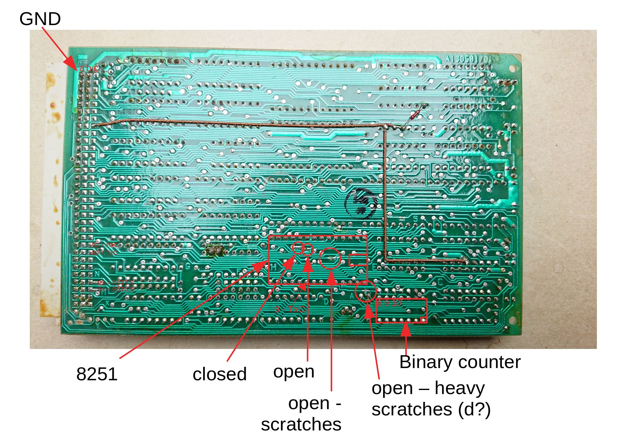
Especially scary is the open jumper with the heavy scratches. It seems to disconnect the TxC signal line (pin 9) of the 8251 from the binary counter output. This might be jumper “d”. That would mean, that there is no clock connected… and hence the 8251 can’t transmit any data.
Unfortunately there are no labels on the jumpers. The jumpers “a”, “b” and “c” seem to be directly at the pins of the counter - at it looks like it would be difficult to not accidentally connecting the wrong pin…
So, the theory for now is: There is no clock. Or the wrong clock.
While researching the clock frequency and which baud rate factor to use, I came across the explanation, why 16x is a common factor: When receiving, the USART chip needs to sample the line and decide, whether it’s asserted or not. In the asynchronous mode, it doesn’t know, when exactly the transmission started, it only knows the baud rate (which needs to match both on the transmitter and receiver). There is only one start bit to signal that now some bits are coming in. The receiver would then know, it needs to sample one bit length later for the first data bit and so on. But depending on how exactly the two independent clocks are on each side, the receiver might be drifting a bit and this would only work, if the two clocks would be perfectly in sync. That’s why typically a oversampling of 16x is used - that way, the receiver chip can basically figure out, where the start bit starts and ends and can choose two sample the data bits in the middle of the bit length - when the signal is most stable.
This is explained in Universalasynchronous receiver-transmitter and discussed in Re: Much Help needed with 8251 USART Problem……..
Pinouts and flow control
I’m always a bit confused about the signal lines and which one is used when and by which end device. Let’s try to clear this up.
You find two different types of connectors: a 25-pin and a 9-pin connector. The null modem cable I made has 25-pins on one end and 9-pins on the other. The Alphatronic has a 25-pin connector, but the USB-to-Serial-Adapter only has the 9-pin variant. Obviously, not all 25 signals are connected.
The serial connection was originally used to connects a modem to a PC. In that sense, a modem is a DCE (Data Circuit-terminating Equipment) and a PC is a DTE (Data Terminal Equipment). DTE connectors are male and DCE connectors are female. When connecting a DCE to a DTE, then a straight cable is used. A null modem cable is needed, when connecting two DTEs or two DCEs together. These cross the Rx/Tx lines and a couple of more lines.
The direction column on RS-232#Pinouts is expressed from the view of the DTE. So, the TxD line is going out, the DTE is sending.
For the sake of simplicity, we’ll now first look at exactly one use case: the Alphatronic is sending and my laptop (using a modern USB-to-Serial adapter) is receiving.
That means, the Alphatronic sends on the TxD signal. It might assert the RTS (Request To Send) signal. It might wait for the CTS (Clear To Send) signal be asserted. That’s also written in the datasheet of 8251: The chip will only transmit, if the CTS signal is asserted (and the transmitter is enabled). So, the CTS signal is important. This is kind of hardware level flow control, which can’t be circumvented. Of course, you can always wire it to be always asserted, so that essentially the hardware flow control is disabled.
The other signal - DSR (Data Set Ready) can be read in the status register. And that’s what the BASIC program does. When the laptop asserts DTR (Data Terminal Ready), then it is received on the other side.
According to Hardware flow control the DTR/DSR lines are used during the entire session and RTS/CTS lines are used for each data block. E.g. the Alphatronic should assert the RTS line to indicate, it wants to send. If the receiving side is ready, it asserts CTS, which then enables the transmitter in 8251 to actually send the data byte.
I’m pretty sure, I tested also the CTS line, as both can be controlled manually in cutecom. And having both asserted didn’t make any different - no byte is transmitted, which supports the theory about the missing clock.
At the beginning of the BASIC program, the command instruction &H13 is issued, which asserts the DTR line, then
the DSR input is checked. Once that is asserted as well, we know the other end is ready and we can proceed to
transmit. In line 260, we again command &H13 - maybe we should assert here RTS as well? Then the command should
be &H33. However, as with manually controlling the CTS line in cutecom, this doesn’t matter.
Next steps
So, how can we figure out, what the real problem is here? There are a couple of things to check:
-
We should double check the connections on the board and figure out where the jumpers are and which jumpers are open or closed. This can be done with a continuity tester and trying to trace the routes. This can then already confirm the theory. And in case, the jumpers are not in the factory default setting, we should then know which jumpers must be soldered open or closed in order to make the serial port work again.
-
We can double check the TxD line with an oscilloscope. In case there is a clock, but it’s the wrong frequency, we could see at least something on that line. However, this is not very likely. While the receiving side (e.g. cutecom) would have seen nothing or garbage, the transmitter should not have been stuck.
-
In the same direction: We could not only check the TxD line, but all the other lines. To see, if there is any activity going on. E.g. can we wiggle the two lines, we can control in software: DTR, RTS?
-
In case the internal clock is really disconnected, we need to provide an external clock. The null modem cable I created doesn’t connect these signal, so we can’t use this. But we can still connect using jumper wires. Then according to the circuit diagram, the TxC/RxC lines are connected via line receivers, so the electric voltage level is the RS232 level (e.g. +/- 12 V). We can connect here e.g. the DTR/DSR signal we can control in software and create a clock. If we are fast enough, we can create a clock suitable for 4800x16. Maybe we need to set the baud rate factor to 1. But when we provide a clock and connect the TxD to RxD, we should be able to receive data. That’s the theory at least.
-
If all that doesn’t help, we would need to check the pins directly on the 8251 chip to see what’s going on. But that’s kind of last resort.
Stay tuned for the next part…
References
- https://adangel.org/2020/04/26/null-modem-cable-alphatronic/
- https://www.f05.uni-stuttgart.de/informatik/fachbereich/computermuseum/
- https://en.wikipedia.org/wiki/RS-232#RTS,_CTS,_and_RTR
- https://en.wikipedia.org/wiki/Flow_control_(data)#Hardware_flow_control
- https://en.wikipedia.org/wiki/Universal_asynchronous_receiver-transmitter
- https://en.wikibooks.org/wiki/Serial_Programming/RS-232_Connections
- https://www.eevblog.com/forum/projects/much-help-needed-with-8251-usart-problem/
Comments
No comments yet.Leave a comment
Your email address will not be published. Required fields are marked *. All comments are held for moderation to avoid spam and abuse.