Alphatronic P2 memory mapping
- Boards assembly
- Memory map
- Switching memory banks
- The plan
- Bank switching routines
- BASIC program
- Results and summary
One last experiment: Since I figured out, that my Alphatronic P2 has an additional 16 kB card (which might make it a P2U), I shall try to use this memory. This is achieved by bank switching.
Boards assembly
As you have seen, the Alphatronic is very modular. There are several different boards that are connected together with a backplane. The cpu (Intel 8085A) is on one card, and on another is RAM. The computermuseum of the University of Stuttgart also has a Alphatronic computer in its collection and they were so kind to put the system documentation of the Alphatronic P1 and P2 computers online on their FTP server: computermuseum.informatik.uni-stuttgart.de/alphatronic/.
There the assembly of the boards is documented:
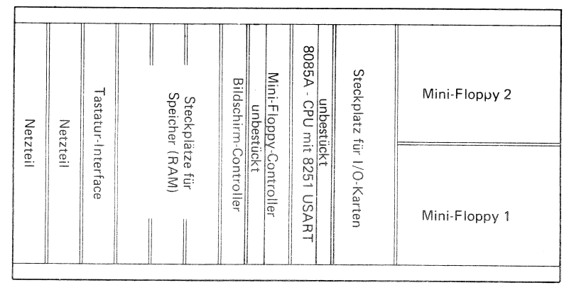
So there are two slots for power supply boards, one for the board interfacing the keyboard (which interestingly has an own micro controller on board: 8041A), three slots for for memory boards (RAM), one slot for the video controller (CRT5037), then an empty slot, the floppy controller, the cpu board, another empty slot and then a free slot for I/O cards. To the right are the two mini floppy drives.
In reality this looks like this:
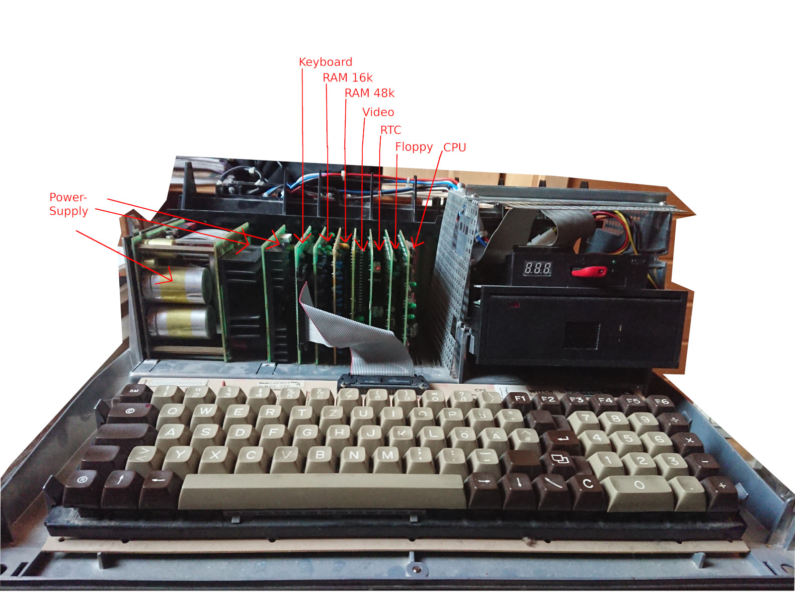
My Alphatronic only has 2 memory boards (16kB and 48kB). It has no I/O cards, but there doesn’t seem to be real space there either. And one floppy drive is a GoTek emulator.
The Alphatronic was available in several models: P1 and P2 and P2 had two flavors: P2S which is P2 but with better floppy drives (double sided), P2U additionally has 64kB of RAM instead of only 48kB.
It seems that my Alphatronic doesn’t fit any of these, it is basically a P2 with extra 16kB or a P2U with single sided floppy drives.
Memory map
In the same system documentation, there is also the complete memory map specified and it is also explained, how to switch the memory banks. Memory bank switching is necessary, since the Alphatronic will boot up from ROM and ROM itself is 6kB+1kB static RAM, so it total the Alphatronic has 48kB + 16kB + 6kB + 1kB memory, which is more than 64kB which is directly addressable by the 16 bit address bus used by 8085A.
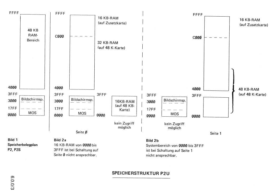
On the left, the memory map of model P2/P2S is displayed. There only the 48kB card is
available. The ROM is mapped from 0x0000 to 0x17ff (6 kB), after that the 1 kB
static RAM is mapped from 0x1800 to 0x1bff. The space between 0x1c00 to 0x2fff
is reserved - probably there is no real memory mapped here. Maybe some other memory
repeats here. The video RAM is mapped from 0x3000 to 0x3fff (4 kB). The 48 kB RAM
is mapped from 0x4000 to 0xffff.
Now for the memory of model P2U, there are two possible states: the initial (boot)
state is like this: The memory from 0x0000 up to 0x3fff is the same: it’s the
ROM (from the 8085A booted) and the video RAM. But the remaining memory is partly
on the 48 kB card, and partly on the 16 kB card. Exactly: 0x4000 to 0xbfff (32 kB)
resides on the 48 kB card, 0xc000 to 0xffff resides on the extra 16 kB card.
This is the status, where I ran all the programs to measure the floppy drive speed.
I located it in Measuring Floppy Drive rotation speed - Part 2
at 0xff00 which is then on the extra 16 kB card. I established already, that this
memory is slower than the memory at 0x1800, which is the static RAM on the CPU card.
Now there is a mechanism (see below) with which one can switch the lower 16 kB
memory space (0x0000 to 0x3fff) with the 16 kB of the memory from the 48 kB, that is
currently not accessible. If that switch is done, then the ROM is not available anymore
until the memory bank is switched back. After the switch, the memory content from 0x4000
to 0xffff stays the same (also physically), only the lower part is swapped.
I wonder, why they decided to split the 48 kB part in that way. There is also a Alphatronic model P1, which has less memory - only 32 kB. But maybe, the P1 and P2 have the same 48 kB card and only P2 has the additional 16 kB card. Due to bank switching, only 32 kB are available together with the default BIOS (MOS) that runs from ROM. That would mean, that the difference between P2 (with 48 kB) and P2U (with 64 kB) is really only software. This is indicated also in the manual “P2U has 64 K-RAM which however can only be leveraged when using the 64 K-CP/M operating system”.
Switching memory banks
For switching memory banks, one has to write a bit combination out to port 0x78.
Switching is as easy as the following assembler sample:
; swap in 16kB - disable system ROM access
mvi a,0x60
out 0x78
; swap out 16kB - enable system ROM access - initial boot state
mvi a,0x20
out 0x78
One interesting note from the manual: “the machine program to switch must be in the address space
above 0x4000 otherwise the program will crash.”
Yes, that’s true: the program counter will continue just after the “out” instruction, but when you have switched the memory, you don’t know, what the next instruction is. So it might do something useful, but more likely it won’t.
Another thing to consider is interrupts: The interrupt vectors for 8085A start at address 0x0000.
After boot, the initial state is, that the system ROM is available at this address, so the reset
interrupt is executed from ROM and the whole system is correctly initialized. But once you have
switched and some other interrupt occurs, it would now not be executed from system ROM but from
this extra 16 kB RAM. So I guess, the 64-K-CP/M system needs to install its own interrupt vector table.
For my simple experiments I hope, I can do without. And still switch back and forth between the memory spaces.
Another side effect: the video RAM is also not available. I assume, the 64-K-CP/M would need to switch
shortly back to update the video RAM in 0x3000-0x3fff. Everytime when something should be printed
on the screen.
The plan
On startup, the MOS (system ROM) is available at 0x0000-0x1fff. I don’t know, whether the BASIC interpreter,
which is loaded at 0x4000 will use the MOS routines e.g. to print to the screen. So I should
be careful when switching the bank and switch it back afterwards. Then hopefully the interpreter
won’t crash. But maybe the interpreter just writes directly into the video RAM at 0x3000.
But that isn’t available either.
In the previous post Alphatronic P2 speed follow-up 2 I already
relocated the floppy index read routine to 0x1800, so I can reuse this. However, I need to switch the memory,
before I poke the routine in, so that it ends up in the correct memory location. After the routine returns,
the BASIC program should switch back the bank.
In the end, I expect that the program will run as slow as at 0xff00 and not as fast as in the static RAM.
If that is the outcome, I can see, that the memory switch worked. I assume, that the memory on the 48 kB card
and the 16 kB card is dynamic RAM which requires a refresh cycle regularly. And this might slow it down.
The machine programs on the 8085A tend to be always memory intensive, since every instruction needs to be loaded
from memory. There is no cache or pipelining involved.
Bank switching routines
The bank switching routines need to be in the upper memory area. I’ll just use 0xff00, which is well known.
I need two routines, one to switch to and another one to switch back. For now, these routines will only
be called from BASIC, but they could also be called from machine code itself (via the CALL instruction).
In any case, the RET instruction needs to be last. It returns to the address that was stored by CALL
in the stack register.
; address       machine code    mnemonic        comments
; swap in 16 kB - ROM is not available afterwards
; ff00          3e 60           mvi a, 0x60
; ff02          d3 78           out 0x78
; ff04          c9              ret

; swap out 16 kB - ROM is available again
; ff05          3e 20           mvi a, 0x20
; ff07          d3 78           out 0x78
; ff09          c9              ret
BASIC program
As always, the BASIC program will poke the machine program into memory and call it. This time, we have three machine programs, we can call.
Important detail: We first need to switch the memory bank, before we poke the machine program “read_index_duration” so that it ends up in the correct memory location.
100 '************** DRIVEROT5
110 CLEAR , &HFF00
120 DEFINT D
130 GOSUB 500 ' install switches
140 CALL SWITCH
150 GOSUB 700 ' install read_index_duration
160 CALL BACK
170 PRINT"In the last used drive a floppy has to be inserted!"
180 INPUT"How many measurements should be taken?"; COUNT
190 DIM DAT%(COUNT)
200 FOR D=0 TO COUNT-1
210     PRINT"  Start measurement ";D
220     CALL SWITCH
230     CALL RID(LOOPS%)
240     CALL BACK
250     DAT%(D)=LOOPS%
260     PRINT"    result:";D;"->";DAT%(D)
270 NEXT
280 PRINT"Data ready"
290 MIN=DAT(0) :MAX=MIN :SUM=0
300 FOR D=0 TO COUNT-1
310     IF DAT(D)<MIN THEN MIN=DAT(D)
320     IF DAT(D)>MAX THEN MAX=DAT(D)
330     SUM=SUM+DAT(D)
340 NEXT
350 MEAN=SUM/COUNT
360 LPS=103448! 'loops per second: 3 MHz/29 cycles - dur. of one loop
370 RPM=INT(60*LPS/MEAN+.5)
380 DIF=MAX-MIN
390 PRINT"  Minimum:";MIN/LPS;"s"
400 PRINT"  Maximum:";MAX/LPS;"s"
410 PRINT"     Mean:";MEAN/LPS;"s"
420 PRINT"Rotations:";RPM;"rpm"
430 PRINT" Accuracy:";DIF*1000/LPS;"ms"
440 END
500 ' Machine programs SWITCH and BACK
510 SWITCH=&HFF00 : BACK=&HFF05
520 I=&HFF00
530    READ D$
540    D=VAL("&H"+D$)
550    IF D>255 THEN RETURN
560    POKE I,D
570    I=I+1
580 GOTO 530
590 DATA 3E,60,D3,78,C9,3E,20,D3,78,C9,E0F
700 ' Machine program RID (=read_index_duration)
710 RID=&H1800
720 I=&H1800
730    READ D$
740    D=VAL("&H"+D$)
750    IF D>255 THEN RETURN
760    POKE I,D
770    I=I+1
780 GOTO 730
790 DATA 3E,D4,D3,50,06,40,11,00,00,DB,50,DB,54
800 DATA A0,CA,0B,18,DB,50,13,DB,54,A0,CA,13,18
810 DATA 73,23,72,C9,E0F
Results and summary
Overall the experiment was not successful. At least, the memory switch seems to do something,
but as soon as the switch occurred, the program hangs. I verified it with some additional PRINT statements.
It just hangs at line 140. Sometimes the MOS restarts with an error code (I guess a warm boot).
But it doesn’t run the BASIC program further.
The hang situation also happens when I directly write to the I/O port from basic, which is possible with the
OUT statement, e.g. OUT &H78, &H60. So actually, I would not have needed to write the little machine program.
Also adding a DI (disable interrupts) into the switch routine and a EI (enable interrupts) when switching
back didn’t help. I’ve inserted it into the machine code, the opcode for DI is 0xF3 and for EI
it is 0xFB. It still hung.
The conclusion is, that the basic interpreter seems to call routines from MOS, the firmware. And as soon this is done - while we have switched the memory banks - we get stuck. Because the firmware is not there. Instead, the 16kB memory is there. And this memory is potentially uninitialized, which means it’s hard to say, what will happen. It probably contains random data. And this random data is executed…
Comments
No comments yet.Leave a comment
Your email address will not be published. Required fields are marked *. All comments are held for moderation to avoid spam and abuse.